Google's Tensor Processing Units power the majority of cutting-edge AI models you interact with daily, yet most engineers remain surprisingly unfamiliar with their architecture. While NVIDIA GPUs dominate developer mindshare, TPUs quietly train and serve Gemini 2.0, Claude, and dozens of other frontier models at scales that would bankrupt most organizations using conventional GPU infrastructure. Anthropic recently committed to deploying over one million TPU chips—representing more than a gigawatt of compute capacity—to train future Claude models.¹ Google's latest Ironwood generation delivers 42.5 exaflops of FP8 compute across 9,216-chip superpods, a scale that redefines what production AI infrastructure means.²
The technical sophistication behind TPUs extends far beyond simple performance metrics. These processors embody a fundamentally different design philosophy than GPUs, trading general-purpose flexibility for extreme specialization in matrix multiplication and tensor operations. Engineers who understand TPU architecture can exploit 256×256 systolic arrays that process 65,536 multiply-accumulate operations per cycle, leverage third-generation SparseCore accelerators for embedding-intensive workloads, and program optical circuit switches that reconfigure multi-petabit datacenter topologies in under 10 nanoseconds.³ The architecture spans everything from transistor-level design decisions to building-scale supercomputer orchestration.
The technical content ahead demands careful attention. We examine seven generations of TPU evolution, dissect systolic array mathematics and dataflow patterns, explore memory hierarchies from SRAM tiles to HBM3e channels, analyze XLA compiler optimizations at the intermediate representation level, and investigate why collective operations execute 10× faster than equivalent Ethernet-based GPU clusters.⁴ You'll encounter register-level specifications, cycle-accurate performance modeling, and the architectural tradeoffs that make TPUs simultaneously more powerful and more constrained than GPUs. The depth here serves engineers building the next generation of AI infrastructure and researchers pushing the boundaries of what current accelerators can achieve.
The Evolution: Seven Generations of Architectural Innovation
TPU v1: Inference-Only Specialization (2015)
Google deployed the first Tensor Processing Unit in 2015 to address a critical problem: neural network inference workloads threatened to double the company's datacenter footprint.⁵ Engineers designed TPU v1 exclusively for inference, removing training capabilities entirely to maximize performance and power efficiency for deployed models. The chip featured a 256×256 systolic array of 8-bit integer multiply-accumulate units, delivering 92 teraops per second at just 28-40 watts thermal design power.⁶
The architecture embodied radical minimalism. A single Matrix Multiply Unit processed INT8 operations through weight-stationary dataflow, where weights remained fixed in the systolic array while activations streamed horizontally across the grid. Partial sums are propagated vertically, eliminating intermediate memory writes for the entire matrix multiplication. The chip, connected to host systems via PCIe, relied on DDR3 DRAM for external memory and operated at 700 MHz—deliberately conservative for power efficiency.⁷
Performance gains astonished even Google's engineers. TPU v1 achieved 30× to 80× improvements in operations per watt compared to contemporary CPUs and GPUs for production inference workloads.⁸ The chip handled Google Search ranking, translation services processing 1 billion daily requests, and YouTube recommendations for 2 billion users. The success validated a core architectural insight: purpose-built accelerators optimized for narrow workloads could deliver order-of-magnitude improvements over general-purpose processors.
TPU v2: Enabling Training at Scale (2017)
The second generation transformed TPUs from inference-only accelerators into complete training platforms. Google redesigned the entire architecture around floating-point operations, replacing the 256×256 INT8 array with dual 128×128 bfloat16 multiply-accumulators per core.⁹ Each chip contained two TensorCores sharing 8GB of High Bandwidth Memory per core, a massive upgrade from DDR3 that provided the bandwidth neural network training demanded.
Bfloat16 precision proved critical for TPU v2's success. The format maintains the same 8-bit exponent range as FP32 while reducing the mantissa to 7 bits, preserving dynamic range for training while halving memory bandwidth requirements.¹⁰ Engineers observed that the reduced mantissa precision actually improved generalization in many models by acting as a form of regularization, while the full FP32 exponent range prevented the underflow and overflow issues that plagued FP16 training.
The architectural innovation that truly differentiated TPU v2 was the Inter-Chip Interconnect (ICI). Previous accelerators required Ethernet or InfiniBand for multi-chip communication, introducing latency and bandwidth bottlenecks. Google designed custom high-speed bidirectional links that connected each TPU directly to four neighbors in a 2D torus topology.¹¹ The interconnect enabled TPU v2 "pods" of up to 256 chips to function as a single logical accelerator, with collective operations like all-reduce executing far faster than network-based alternatives.
TPU v3: Water-Cooled Performance Scaling (2018)
Google pushed clock speeds and core counts aggressively in TPU v3, delivering 420 teraflops per chip—more than doubling v2's performance.¹² The increased power density forced a dramatic architectural change: liquid cooling. Each TPU v3 pod required water cooling infrastructure, a departure from the air-cooled designs of previous generations and most datacenter accelerators.¹³
The chip maintained the dual 128×128 MXU architecture but increased the total number of cores and improved memory bandwidth. Each TPU v3 contained four chips with two cores each, sharing 32GB of HBM memory total across the chips.¹⁴ The vector processing units received enhancements for activation functions, normalization operations, and gradient computations that frequently bottlenecked training on the matrix units alone.
Deployments scaled to 2,048-chip pods using the same 2D torus ICI topology as v2 but with increased per-link bandwidth. Google trained increasingly large models on v3 pods, discovering that the torus topology's reduced network diameter (maximum distance between any two chips scales as N/2 rather than N) minimized communication overhead for both data-parallel and model-parallel training strategies.¹⁵
TPU v4: Optical Circuit Switching Breakthrough (2021)
The fourth generation represented Google's most significant architectural leap since the original TPU. Engineers increased pod scale to 4,096 chips while introducing optical circuit switching (OCS) for interconnect, a technology borrowed from telecommunications that revolutionized datacenter-scale ML infrastructure.¹⁶
TPU v4's core architecture featured four 128×128 MXUs per TensorCore alongside enhanced vector and scalar units. Each TensorCore pair shared 128MB of Common Memory in addition to per-core Vector Memory, enabling more sophisticated data staging and reuse patterns.¹⁷ The chip topology evolved from 2D to 3D torus, connecting each TPU to six neighbors rather than four, further reducing network diameter and improving bisection bandwidth.
The optical circuit switching system changed everything about large-scale deployment. Rather than fixed cabling between TPUs, Google deployed programmable optical switches that could dynamically reconfigure which chips connected to which. MEMS (microelectromechanical systems) mirrors physically redirect light beams to patch arbitrary TPU pairs together, introducing essentially zero latency beyond the optical fiber transmission time.¹⁸ The switches reconfigure in sub-10-nanosecond windows, faster than most network protocol handshakes.
The OCS architecture enabled capabilities previously impossible. Google could provision "slices" of any size, from four chips to the full 4,096-chip pod, by programming the optical switches appropriately. Failed chips could be seamlessly routed around without taking down entire racks. Most remarkably, physically distant TPUs in different datacenter locations could be logically adjacent in the network topology, decoupling physical and logical layout entirely.¹⁹
TPU v4 also introduced SparseCore, a specialized processor for handling embedding operations used every day in recommendation systems, ranking models, and large language models with massive vocabulary embeddings. The SparseCore featured four dedicated processors per chip, each with 2.5MB of scratchpad memory and optimized dataflow for sparse memory access patterns.²⁰ Models with ultra-large embeddings achieved 5-7× speedups using just 5% of total chip die area and power budget.
TPU v5p and v5e: Specialization and Scale (2022-2023)
Google split the fifth generation into two distinct products targeting different use cases. TPU v5p prioritized maximum performance for large-scale training, while v5e optimized for cost-effective inference and smaller training jobs.²¹
TPU v5p achieved approximately 4.45 exaflops per second across 8,960-chip pods, more than doubling v4's maximum pod size.²² The interconnect bandwidth reached 4,800 Gbps per chip, and the 3D torus topology connected chips in massive 16×20×28 superpods. The optical circuit switching fabric managed 13,824 optical ports across 48 OCS units to wire a complete v5p superpod, representing one of the largest production optical switching deployments in computing history.²³
TPU v5e took a different approach, reducing core count and clock speed to hit aggressive power and cost targets. Inference-optimized chips contained only one TPU core per chip rather than two, and returned to the 2D torus topology, which was sufficient for smaller pod sizes.²⁴ The architectural simplification enabled Google to price v5e competitively for workloads where absolute performance mattered less than performance per dollar.
TPU v6e Trillium: Quadrupling Matrix Performance (2024)
Trillium marked another architectural inflection point by expanding the Matrix Multiply Unit from 128×128 to 256×256 multiply-accumulators.²⁵ The larger array quadrupled FLOPs per cycle at the same clock speed, delivering 4.7× the peak compute performance of TPU v5e through a combination of the expanded MXU and increased clock frequencies.
The memory subsystem received equally dramatic upgrades. HBM capacity doubled to 32GB per chip, with bandwidth doubled by next-generation HBM channels.²⁶ The Interchip Interconnect bandwidth similarly doubled, enabling pods of 256 Trillium chips to sustain higher throughput for models that stressed both compute and communication.²⁷
Trillium featured the third-generation SparseCore accelerator, with enhanced capabilities for ultra-large embeddings in ranking and recommendation workloads. The updated design improved memory access patterns and increased the adequate bandwidth between SparseCores and HBM for models dominated by embedding lookups rather than matrix multiplications.²⁸
Energy efficiency improved by 67% over v5e despite substantial performance gains.²⁹ Google achieved the efficiency gains through advanced process nodes, architectural optimizations that reduced wasted work, and careful power gating of unused units during operations that didn't stress all parts of the chip simultaneously.
TPU v7 Ironwood: The FP8 Era (2025)
Google's seventh-generation TPU, codenamed Ironwood, represents the first TPU designed with native FP8 support and optimized specifically for the "age of inference" while maintaining state-of-the-art training performance.³⁰ Each Ironwood chip delivers 4.6 petaFLOPS of dense FP8 compute—slightly exceeding NVIDIA's competing B200 at 4.5 petaFLOPS—while pulling 600W thermal design power.³¹
The memory system expanded to 192GB of HBM3e memory per chip, six times Trillium's capacity, with bandwidth reaching 7.4TB/s.³² The dramatic memory increase enables serving ultra-large models with key-value caches that previously required complex tensor parallelism across multiple accelerators. Google specifically designed the memory capacity to support emerging multi-modal models and long-context applications approaching million-token windows.
Ironwood's interconnect provides 9.6 Tbps of aggregate bidirectional bandwidth through four ICI links, translating to 1.2 TB/s of peak per-chip bandwidth.³³ The architecture scales from 256-chip pods for smaller deployments to massive 9,216-chip superpods delivering 42.5 FP8 exaflops of compute power.³⁴ Google's Jupiter datacenter network technology could theoretically support up to 43 Ironwood superpods in a single cluster—roughly 400,000 accelerators representing an almost incomprehensible scale of compute.³⁵
The FP8 support represents a fundamental shift in precision strategy. Prior TPU generations emulated 8-bit operations using software techniques, which introduced overhead. Ironwood implements native FP8 multiply-accumulate units supporting both E4M3 (4-bit exponent, 3-bit mantissa) and E5M2 (5-bit exponent, 2-bit mantissa) formats.³⁶ The dual format support enables mixing E4M3 for forward passes where precision matters less and E5M2 for backward passes where maintaining gradient magnitudes prevents training instability.
Anthropic's commitment to deploy over one million Ironwood chips beginning in 2026 demonstrates the architecture's production readiness. The company plans to leverage well over a gigawatt of TPU capacity—enough to power a small city—exclusively for training and serving Claude models.³⁷ The scale dwarfs even the most significant known GPU deployments and represents a fundamental bet on TPU architecture for frontier model development.
Current-Generation Quick Reference
The following tables provide scannable specifications for the three current-generation TPUs most relevant to production deployments in 2025:
Table 1: Core Compute Specifications
[caption id="" align="alignnone" width="1386"] SpecificationTPU v5eTPU v5pTPU v6e (Trillium)TPU v7 (Ironwood) MXU Array Size 128×128 128×128 256×256 256×256 MACs per Cycle 16,384 16,384 65,536 65,536 Peak BF16 TFLOPS ~197 ~459 ~918 ~2,300 (est.) Peak FP8 PFLOPS N/A (emulated) N/A (emulated) N/A (emulated) 4.6 Native Precision BF16, INT8 BF16, INT8 BF16, INT8 BF16, FP8, INT8 TensorCores/Chip 1 2 1 1 [/caption]
Table 2: Memory and Bandwidth
[caption id="" align="alignnone" width="1380"]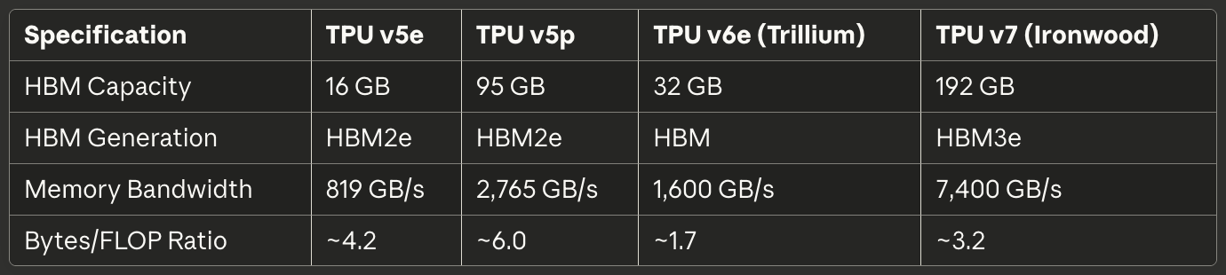 SpecificationTPU v5eTPU v5pTPU v6e (Trillium)TPU v7 (Ironwood) HBM Capacity 16 GB 95 GB 32 GB 192 GB HBM Generation HBM2e HBM2e HBM HBM3e Memory Bandwidth 819 GB/s 2,765 GB/s 1,600 GB/s 7,400 GB/s Bytes/FLOP Ratio ~4.2 ~6.0 ~1.7 ~3.2 [/caption]
Table 3: Interconnect and Scaling
[caption id="" align="alignnone" width="1384"]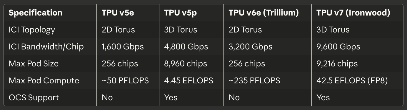 SpecificationTPU v5eTPU v5pTPU v6e (Trillium)TPU v7 (Ironwood) ICI Topology 2D Torus 3D Torus 2D Torus 3D Torus ICI Bandwidth/Chip 1,600 Gbps 4,800 Gbps 3,200 Gbps 9,600 Gbps Max Pod Size 256 chips 8,960 chips 256 chips 9,216 chips Max Pod Compute ~50 PFLOPS 4.45 EFLOPS ~235 PFLOPS 42.5 EFLOPS (FP8) OCS Support No Yes No Yes [/caption]
Table 4: Power and Efficiency
[caption id="" align="alignnone" width="1380"] SpecificationTPU v5eTPU v5pTPU v6e (Trillium)TPU v7 (Ironwood) TDP ~120-200W ~250-300W ~120-200W 600W Cooling Air Liquid Air Liquid TFLOPS/Watt (BF16) ~1.0-1.6 ~1.5-1.8 ~4.6-7.7 ~3.8 Energy vs Prior Gen Baseline N/A 67% better than v5e 2× better than Trillium [/caption]
Table 5: Recommended Use Cases
[caption id="" align="alignnone" width="1382"] Use Case Best Choice Rationale Cost-optimized inference TPU v5e: Lowest cost per inference query Large-scale training (>1000 chips) TPU v5p or Ironwood 3D torus + OCS enables massive pods Medium training jobs (256 chips) TPU v6e Trillium Best perf/watt, 4.7× compute vs v5e Memory-bound models (>70B params), Ironwood 192GB HBM enables larger batch sizes Long-context inference (>100K tokens) Ironwood HBM capacity supports massive KV caches Embedding-heavy workloads TPU v5p or Ironwood SparseCore + large HBM [/caption]
## Hardware Architecture: Inside the Silicon
Systolic Array Mathematics and Dataflow
The Matrix Multiply Unit forms the heart of TPU architecture, and understanding systolic arrays requires grasping their fundamentally different approach to parallelism compared to GPU SIMD lanes. A systolic array chains multiply-accumulate units in a grid where data flows rhythmically through the structure—hence "systolic," evoking the rhythmic pumping of blood through the heart.³⁸
Consider TPU v6e's 256×256 systolic array performing the matrix multiplication C = A × B. Engineers preload the weights of matrix B into the 65,536 individual multiply-accumulate units arranged in a grid. Matrix A's activation values enter from the left edge and flow horizontally across the array. Each MAC unit multiplies its stored weight by the incoming activation, adds the result to a partial sum arriving from above, and passes both the activation (horizontally) and updated partial sum (vertically) to neighboring units.³⁹
The dataflow pattern means each activation value gets reused 256 times as it traverses the horizontal dimension, and each partial sum accumulates contributions from 256 multiplications as it flows vertically. Critically, all intermediate results pass directly between adjacent MAC units via short wires rather than round-tripping to memory. The architecture performs 65,536 multiply-accumulate operations every clock cycle, and during the entire matrix multiplication involving potentially millions of operations, zero intermediate values touch DRAM or even on-chip SRAM.⁴⁰
The weight-stationary dataflow pattern optimizes for the most common case in neural network inference and training: repeatedly multiplying many different activation matrices by the same weight matrix. Engineers load weights once, then stream unbounded activation batches through the array without reloading. The pattern works exceptionally well for convolutional layers, fully connected layers, and the Q·K^T and attention·V operations that dominate transformer models.⁴¹
Energy efficiency stems from data reuse and spatial locality. Reading a value from DRAM consumes roughly 200× as much energy as a single multiply-accumulate operation.⁴² By reusing each weight 256 times and each activation 256 times without memory accesses, the systolic array achieves operations-per-watt ratios impossible for architectures that shuttle data back and forth between compute units and memory hierarchies.
The systolic array's weakness emerges with dynamic or irregular computation patterns. Because data flows through the grid on a fixed schedule, the architecture struggles with conditional execution, sparse matrices (unless using SparseCore), and operations that require random access patterns. The inflexibility trades generality for extreme efficiency on its target workload: dense matrix multiplication with predictable access patterns.
TensorCore Internal Architecture
Each TPU chip contains one or more TensorCores—the complete processing unit comprising the Matrix Multiply Unit, Vector Processing Unit, and Scalar Unit working in concert.⁴³ The TensorCore represents the fundamental building block that software targets, and understanding the interaction between its three components explains both TPU performance characteristics and programming patterns.
The Matrix Multiply Unit executes 16,000 multiply-accumulate operations per cycle on bfloat16 or FP8 inputs with FP32 accumulation.⁴⁴ The mixed-precision approach preserves numerical accuracy in the accumulator while reducing memory bandwidth for inputs. Engineers observed that maintaining complete FP32 precision during accumulation prevents catastrophic cancellation errors when summing hundreds or thousands of intermediate products, while reduced-precision inputs rarely affect final model quality.
The Vector Processing Unit handles operations poorly suited to the MXU's rigid structure. Activation functions (ReLU, GELU, SiLU), normalization layers (batch norm, layer norm), softmax, pooling, dropout, and element-wise operations execute on the VPU's 128-lane SIMD architecture.⁴⁵ The VPU operates on FP32 and INT32 datatypes, providing the precision required for numerically sensitive operations like softmax, where exponentials and divisions can create large dynamic ranges.
The Scalar Unit orchestrates the entire TensorCore. The single-threaded processor executes control flow, calculates memory addresses for complex indexing patterns, and initiates DMA transfers from High Bandwidth Memory to Vector Memory.⁴⁶ Because the scalar unit runs single-threaded, each TensorCore can create only one DMA request per cycle—a bottleneck for memory-intensive operations that don't saturate the MXU or VPU compute throughput.
The memory hierarchy feeding the TensorCore determines achievable performance as much as raw compute capability. Vector Memory (VMEM) acts as a software-managed scratchpad SRAM exclusive to each TensorCore, typically sized at tens of megabytes. The XLA compiler explicitly schedules data movement between HBM and VMEM, deciding what to stage into the fast local memory and when to write results back.⁴⁷
Common Memory (CMEM), present in TPU v4 and later generations, provides a larger shared pool accessible to all TensorCores on a chip. The TPU v4 architecture allocated 128MB of CMEM shared between two TensorCores, enabling more sophisticated producer-consumer patterns in which one core's outputs feed another core's inputs without round-tripping to HBM.⁴⁸.
The programming model implications matter enormously. Because the scalar unit single-threads and the vector memory require explicit management, TPU programming resembles 1990s-era embedded systems development more than modern GPU programming. CUDA abstracts memory movement with unified memory and hardware-managed caches; TPU code (whether generated by XLA or written by hand in Pallas) must explicitly orchestrate every data transfer. Manual control enables expert optimization but raises the bar for competent performance.
High Bandwidth Memory Architecture
Modern TPUs use HBM (High Bandwidth Memory), or HBM3e, a radically different memory technology from the DDR SDRAM found in CPUs, and the GDDR used in many GPUs. HBM stacks multiple DRAM dies vertically using through-silicon vias (TSVs), then places the stack directly adjacent to the processor die on a silicon interposer.⁴⁹ The short electrical path and wide interface enable dramatically higher bandwidth than conventional memory technologies.
TPU v7 Ironwood implements 192GB of HBM3e with a total bandwidth of 7.4 TB/s.⁵⁰ The memory system is divided into multiple channels, each providing independent access to a separate portion of the total capacity. The XLA compiler and runtime must carefully partition tensors across HBM channels to maximize parallel access and avoid hotspots where one channel saturates while others sit idle.
The memory interface width dwarfs conventional DRAM. Where a DDR5 channel might provide 64 bits of width, an HBM channel typically spans 1,024 bits.⁵¹ The extreme width enables high bandwidth at relatively modest clock speeds, reducing power consumption and signal integrity challenges compared to pushing narrow interfaces to multi-gigahertz frequencies.
Latency characteristics differ substantially from GPU memory systems. TPUs lack hardware-managed caches beyond small local buffers, so the architecture relies on software explicitly staging data into VMEM well before compute units need it. The lack of caches means memory latency directly impacts performance unless the compiler successfully hides latency through prefetching and double-buffering.⁵²
Memory capacity limits dominate many workloads more than compute throughput. A 175-billion parameter model with bfloat16 weights requires 350GB to store parameters—already exceeding Ironwood's 192GB HBM even before accounting for activations, optimizer states, or gradient buffers. Training such models demands sophisticated techniques like gradient checkpointing, optimizer state sharding across multiple chips, and careful scheduling of parameter updates to minimize memory footprint.⁵³
The TPU runtime enforces specific tensor layout requirements to maximize MXU efficiency. Because the systolic array processes data in 128×8 tiles, tensors should align to these dimensions to avoid padding waste.⁵⁴ Poorly sized matrices force the hardware to process partial tiles with MACs sitting idle, directly reducing FLOPS utilization. The compiler attempts to pad and reshape tensors automatically, but conscious layout choices in the model architecture can substantially improve performance.
SparseCore: Specialized Embedding Acceleration
While the Matrix Multiply Unit excels at dense matrix operations, embedding-intensive workloads exhibit radically different characteristics. Recommendation models, ranking systems, and large language models frequently access massive embedding tables (often hundreds of gigabytes) through irregular, data-dependent indices. The MXU's structured dataflow provides no advantage for these sparse memory access patterns, motivating SparseCore's specialized architecture.⁵⁵
SparseCore implements a tiled dataflow processor fundamentally different from the MXU's systolic array. TPU v4 featured four SparseCores per chip, each containing 16 compute tiles.⁵⁶ Each tile operates as an independent dataflow unit with local scratchpad memory (SPMEM) and processing elements. The tiles execute in parallel, processing disjoint subsets of embedding operations simultaneously.
The memory hierarchy places hot data in small, fast SPMEM while keeping the full embedding tables in HBM. The XLA compiler analyzes embedding access patterns to determine which embedding vectors merit caching in SPMEM versus fetching on demand from HBM.⁵⁷ The strategy resembles traditional CPU cache hierarchies, but with software rather than hardware making placement decisions.
SparseCores connect directly to HBM channels, bypassing the TensorCore's memory path entirely. The dedicated connection prevents embedding operations from competing with dense matrix operations for memory bandwidth, enabling both to proceed in parallel.⁵⁸ The partitioning works exceptionally well for models like Deep Learning Recommendation Models (DLRMs) that interleave dense neural network layers with large embedding lookups.
The mod-sharding strategy distributes embeddings across SparseCores by computing target_sc_id = col_id % num_total_sparse_cores.⁵⁹ The simple sharding function ensures load balancing when embedding IDs are distributed uniformly, but can create hotspots for skewed access patterns. Engineers working with real-world data often need to analyze embedding frequency distributions and manually rebalance sharding to avoid bottlenecks.
Performance gains from SparseCore reach 5-7× compared to implementing identical operations on the MXU and VPU, while consuming only 5% of chip die area and power.⁶⁰ The dramatic efficiency advantage stems from purpose-building the dataflow for sparse operations rather than forcing them through dense matrix infrastructure. The specialization principle applies recursively within TPU architecture: just as TPUs specialize beyond GPUs' general-purpose design, SparseCores specialize beyond TPUs' matrix-oriented design.
Trillium's third-generation SparseCore introduced variable SIMD width (8 elements for FP32, 16 for bfloat16) and improved memory access patterns, reducing wasted bandwidth from misaligned reads.⁶¹ The architectural evolution demonstrates Google's continued investment in embedding acceleration as large language models trend toward larger vocabularies and more sophisticated retrieval-augmented generation patterns.
Interconnect Technology: Wiring the Supercomputer
Inter-Chip Interconnect (ICI) Architecture
The Inter-Chip Interconnect is the critical technology that enables TPUs to function as unified supercomputers rather than isolated accelerators. Unlike GPUs that communicate through Ethernet or InfiniBand networks, ICI implements custom high-speed serial links directly connecting neighboring TPUs with microsecond-scale latency and terabit-per-second bandwidth.⁶²
Topology evolution across TPU generations reflects changing requirements for pod scaling. TPU v2, v3, v5e, and v6e implement 2D torus topologies in which each chip connects to its four nearest neighbors (north, south, east, and west).⁶³ The links wrap around at boundaries, creating a donut-shaped logical topology that eliminates edge chips with fewer connections. A 16×16 grid of 256 TPUs thus provides uniform bandwidth and latency characteristics regardless of which two chips communicate.
TPU v4 and v5p upgraded to 3D torus topologies with each chip connecting to six neighbors.⁶⁴ The additional dimension reduces network diameter—the maximum hop count between any two chips—from roughly 2√N to 3∛N. For a 4,096-chip pod, the maximum hops drop from approximately 128 to 48, substantially reducing worst-case communication latency for globally synchronizing operations such as all-reduce.
The toroidal structure delivers another critical advantage: equal bisection bandwidth regardless of how workloads partition across chips. Any cut that divides the torus in half crosses the same number of links, preventing pathological cases where poor job placement creates network bottlenecks.⁶⁵ The uniform bisection bandwidth simplifies scheduling and enables the optical circuit switch reconfigurability discussed below.
Bandwidth specifications scale impressively across generations. TPU v6e provides 13 TB/s of ICI bandwidth per chip.⁶⁶ TPU v5p reached 4,800 Gbps per chip across six 3D torus links.⁶⁷ Ironwood implements four ICI links with a 9.6 Tbps aggregate bidirectional bandwidth, translating to 1.2 TB/s per chip.⁶⁸ For comparison, a top-tier 400GbE network interface provides 50GB/s bidirectional bandwidth—an order of magnitude less than modern TPU ICI.
Link technology within racks uses direct-attached copper (DAC) cables for short distances between chips in the same 4×4×4 cube.⁶⁹ The copper connections minimize cost and power while providing the required bandwidth for tightly coupled chips executing synchronized operations. Inter-cube and pod-scale links transition to optical transceivers, trading higher cost and power for the distance and bandwidth needed to span datacenter racks.
Collective operations exploit ICI's unique properties. All-reduce, all-gather, and reduce-scatter operations frequently synchronize activations and gradients across chips during training. On Ethernet-based GPU clusters, these collectives traverse a hierarchical network with switches, cables, and network interface cards, introducing latency at each hop. TPU ICI implements optimized collective algorithms directly in hardware, executing all-reduce operations 10× faster than equivalent Ethernet-based GPU implementations.⁷⁰
Optical Circuit Switching: Dynamic Topology Reconfiguration
Google's deployment of optical circuit switching (OCS) with TPU v4 represented one of the most significant innovations in datacenter networking in decades. Traditional packet-switched networks—whether Ethernet or InfiniBand—establish logical connections by routing packets hop-by-hop through switches that examine headers and forward to appropriate output ports. OCS instead uses programmable optical elements to create direct physical light paths between endpoints, eliminating switching latency entirely.⁷¹
The core technology relies on MEMS (microelectromechanical systems) mirrors that physically rotate to redirect light beams. A transmitter on TPU A sends light into the OCS. Tiny mirrors inside the OCS rotate to reflect that light beam to a receiver on TPU B. The connection becomes a direct optical path from A to B with essentially zero added latency beyond light propagation through the fiber.⁷²
Reconfiguration speed determines the practicality of OCS in production systems. Google's deployment achieves sub-10-nanosecond switching times—faster than typical network protocol round-trip times.⁷³ The reconfiguration speed enables dynamic topology changes matching workload requirements without disrupting running jobs or requiring carefully coordinated traffic engineering.
TPU v5p demonstrated OCS at a massive scale. The architecture uses optical circuit switches that deliver four petabits per second of aggregate bandwidth across the switching fabric.⁷⁴ A single v5p superpod requires 48 OCS units managing 13,824 optical ports to wire 8,960 chips in the 16×20×28 3D torus configuration.⁷⁵ The switching system represents one of the largest optical networking deployments in any computing environment.
OCS provides capabilities impossible with traditional networks. Physical topology and logical topology fully decouple—two TPUs in opposite corners of the datacenter appear as adjacent neighbors if the OCS creates direct optical paths. Failed chips or links get routed around by reprogramming mirrors to exclude faulty components and maintain the logical torus structure. New jobs receive "slices" of any size by programming the OCS to create appropriate pod configurations without physically re-cabling racks.⁷⁶
The architecture integrates with Google's Jupiter data center network to scale beyond a single pod. Jupiter delivers multi-petabit-per-second bisection bandwidth across entire datacenters using Google's custom silicon switches and control plane.⁷⁷ Multiple TPU superpods connect via Jupiter fabric, theoretically supporting clusters of up to 400,000 accelerators if network capacity permits.⁷⁸
Power consumption and reliability characteristics favor optical circuit switching for TPU-scale deployments. Traditional packet switches consume substantial power processing and forwarding packets at terabit-per-second rates. OCS switches consume power only to operate MEMS mirrors during reconfiguration events, then sit idle, passing light with minimal loss while connections remain stable.⁷⁹ The architecture's simplicity improves reliability by eliminating complex packet processing and buffering logic prone to bugs and performance anomalies.
Pod Architecture and Scaling Characteristics
TPU pods represent the largest single unit of TPUs connected through ICI, forming a unified accelerator. The physical structure builds hierarchically from individual chips to trays to cubes to racks to complete pods.⁸⁰ Understanding the hierarchy matters for reasoning about memory capacity, communication bandwidth, and fault tolerance at different scales.
The fundamental building block consists of four chips on a single tray connected to a host CPU via PCIe.⁸¹ The PCIe connection handles control plane operations, initial program loading, and infeed/outfeed for training data and inference results. The actual inter-chip communication for distributed training flows through ICI rather than PCIe, avoiding PCIe bandwidth bottlenecks.
Sixteen trays (64 chips) form a single 4×4×4 cube—the basic unit for pod construction. Within a cube, all ICI connections use direct-attached copper cables since chips reside in the same rack with short physical distances.⁸² The cube implements a complete 3D torus with wrap-around connections, creating a self-contained 64-chip unit that could theoretically operate independently.
TPU v4 pods scale to 64 cubes totaling 4,096 chips.⁸³ The inter-cube connections transition to optical links managed by the optical circuit switching fabric. The OCS can provision these 4,096 chips as a single enormous pod, multiple smaller independent pods, or dynamically reconfigure mid-job if required. The flexibility enables datacenter operators to balance utilization across different job sizes and priorities.
TPU v5p pushed pod scale to 8,960 chips in a 16×20×28 3D torus.⁸⁴ The specific dimensions reflect careful bandwidth and diameter optimization—prime factorizations matter for network topology! The pod delivers 4.45 exaflops of compute and represents one of the largest single-pod configurations deployed in production.
Ironwood supports both 256-chip pods for smaller deployments and 9,216-chip superpods for massive frontier model training.⁸⁵ The 9,216-chip configuration delivers 42.5 FP8 exaflops—more compute than the entire Top500 list of supercomputers contained just five years earlier.⁸⁶ The scale redefines what organizations can accomplish with synchronous training rather than pipelined or asynchronous approaches.
Scaling efficiency determines whether larger pods actually help. Communication overhead increases with pod size as chips spend more time synchronizing rather than computing. Google Research published results demonstrating 95% scaling efficiency at 32,768 TPUs for specific workloads, meaning 32,768 TPUs delivered 95% of the performance that perfect linear scaling would predict.⁸⁷ The efficiency stems from hardware-accelerated collectives, optimized compiler transformations, and clever algorithmic approaches to reduce gradient synchronization frequency.
Fault tolerance at the pod scale requires sophisticated handling. Statistical probability guarantees component failures in any system with thousands of chips running continuously. The optical circuit switch enables graceful degradation by reconfiguring around failed components. Training checkpointing occurs at regular intervals (typically every few minutes), so job failure requires restarting only from the last checkpoint rather than from scratch.⁸⁸
Software Stack: Compilers, Frameworks, and Programming Models
XLA Compiler: Optimizing Computation Graphs
XLA (Accelerated Linear Algebra) forms the foundation of TPU's software stack, compiling high-level framework operations into optimized machine code for execution on the TPU.⁸⁹ The compiler implements aggressive optimizations impossible in general-purpose compilers because it exploits domain knowledge about machine learning workloads and TPU architecture characteristics.
Fusion represents XLA's most impactful optimization. The compiler analyzes computation graphs to identify sequences of operations that can execute without materializing intermediate tensors. A simple example: element-wise operations like relu(batch_norm(conv(x))) normally require writing the convolution output to memory, reading it for batch normalization, writing that result to memory, and reading again for ReLU. XLA fuses these operations into a single kernel that produces the final ReLU output without intermediate memory traffic.⁹⁰
Fusion's impact scales with TPU's architecture. Memory bandwidth constrains many workloads more than compute throughput—the MXU can perform matrix multiplications faster than the memory system can feed it data. Eliminating intermediate memory writes and reads through fusion directly translates to performance improvements, often delivering 2× or more speedup for activation-function-heavy networks.⁹¹
Memory layout transformations optimize tensor storage for hardware requirements. Neural networks often represent tensors in the NHWC format (batch, height, width, channels) for intuitive indexing, but TPU MXUs perform best with layouts that align with 128×8 tiles.⁹² XLA automatically transposes, reshapes, and pads tensors to match hardware preferences, inserting layout transformations only where necessary and sometimes propagating preferred layouts backward through the graph to minimize total transformation overhead.
The compiler implements sophisticated constant folding and dead code elimination. ML graphs frequently contain subgraphs whose outputs depend only on constants—batch normalization parameters, inference dropout rates, and shape calculations that can be executed once rather than per batch. XLA evaluates these subgraphs at compile time and replaces them with constant tensors, reducing runtime work.⁹³
Cross-replica optimization exploits knowledge about distributed execution. When training across multiple TPU cores, certain operations (like batch normalization statistics) require aggregation across all replicas. XLA identifies these patterns and generates optimized collective operations that exploit ICI's hardware-accelerated all-reduce rather than implementing aggregation through explicit message passing.⁹⁴
The compiler targets an intermediate representation, Mosaic, specifically for TPUs. Mosaic operates at a higher abstraction level than assembly language but lower than the input computation graph. The language exposes TPU architectural features, such as systolic arrays, vector memory, and VMEM staging, while hiding low-level details, such as instruction scheduling and register allocation.⁹⁵
Auto-tuning capabilities select optimal tile sizes and operation parameters through empirical search. The XLA Auto-Tuning (XTAT) system tries different fusion strategies, memory layouts, and tile dimensions, profiles each variant's performance, and selects the fastest configuration.⁹⁶ The search can require substantial compile time for complex models, but produces dramatic runtime speedups by discovering counter-intuitive optimizations humans rarely identify manually.
JAX: Composable Transformations and SPMD
JAX provides a NumPy-compatible interface for numerical computation with automatic differentiation, JIT compilation to XLA, and first-class support for program transformation.⁹⁷ The framework's functional programming paradigm and composable transformation model align naturally with TPU execution models and distributed parallelism patterns.
The core JAX abstraction applies mathematical transformations to functions. Grad (f) computes f's gradient. Jit (f) JIT-compiles f to XLA. vmap(f) vectorizes f over a new dimension. Critically, transformations compose: jit(grad(vmap(f))) works exactly as expected, compiling a vectorized gradient function.⁹⁸ The compositional model enables building complex distributed training loops from simple, testable components.
SPMD (Single Program, Multiple Data) represents JAX's distributed execution model. Programmers write code as if targeting a single device, then add sharding annotations indicating how to partition tensors across multiple TPU cores. The XLA compiler and GSPMD (General SPMD) subsystem automatically insert communication operations to maintain program semantics while executing across distributed devices.⁹⁹
Sharding annotations use PartitionSpec to declare distribution strategies. PartitionSpec('batch', None) shards a tensor's first dimension across the 'batch' axis of the device mesh while replicating the second dimension. PartitionSpec(None, 'model')implements tensor parallelism by partitioning the second dimension. The annotations can be composed with arbitrary tensor ranks and device mesh dimensions.¹⁰⁰
GSPMD's automatic parallelization eliminates vast amounts of boilerplate code. Traditional distributed training requires manually inserting an all-gather before operations that need full tensors, a reduce-scatter after computing distributed gradients, and an all-reduce for global reductions. GSPMD analyzes sharding specifications and automatically inserts appropriate collectives, freeing programmers to focus on the algorithm rather than communication engineering.¹⁰¹
The compiler propagates sharding decisions through the computation graph using constraint solving. If operation A outputs a sharded tensor consumed by operation B, GSPMD infers B's optimal sharding based on how the output gets used, potentially inserting resharding operations only where mathematically necessary.¹⁰² The automated inference prevents the "sharding spaghetti" that plagues hand-written distributed code.
JAX provides fine-grained control when automation falls short. with_sharding_constraint forces specific sharding at graph locations, overriding automatic inference. Custom PJIT (parallel JIT) annotations specify exact device placement and sharding strategies for performance-critical code paths. The layered model enables rapid prototyping with automatic sharding while supporting expert optimization where required.¹⁰³
Shardy emerged as GSPMD's successor in 2025, implementing improved constraint propagation algorithms and better handling of dynamic shapes.¹⁰⁴ The new system exposes additional optimization opportunities by reasoning about sharding choices jointly across larger graph regions rather than operation-by-operation.
PyTorch/XLA: Bringing PyTorch to TPUs
PyTorch/XLA enables running PyTorch models on TPUs with minimal code changes, bridging the gap between PyTorch's imperative programming model and XLA's graph-based compilation.¹⁰⁵ The integration balances preserving PyTorch's developer experience with exposing TPU-specific optimizations.
The fundamental challenge stems from PyTorch's eager execution philosophy. PyTorch executes operations immediately as Python statements execute, enabling debugging with standard tools and natural control flow. XLA requires capturing complete computation graphs before compilation, creating tension between eager execution and the performance benefits of graph compilation.¹⁰⁶
PyTorch/XLA 2.4 introduced eager mode support, addressing the impedance mismatch. The implementation dynamically traces PyTorch operations into XLA graphs, allowing developers to write standard PyTorch code while still benefiting from XLA compilation.¹⁰⁷ The mode trades some compilation optimization opportunities for development velocity and debugging simplicity.
Graph mode remains the primary path for production deployments. Developers explicitly mark functions for XLA compilation using decorators or compilation APIs. The explicit annotations enable aggressive optimization but require understanding which operations should be fused into a single XLA graph versus executed independently.¹⁰⁸
Pallas integration brings custom kernel development to PyTorch/XLA. Pallas provides a low-level language for writing TPU kernels when XLA's automatic fusion falls short or specialized operations require hand-optimization.¹⁰⁹ The language exposes TPU memory hierarchy (VMEM, CMEM, HBM) and compute units (MXU, VPU) while remaining higher-level than raw assembly.
Built-in Pallas kernels implement performance-critical operations like FlashAttention and PagedAttention. FlashAttention's tiled attention computation reduces memory bandwidth requirements from O(n²) to O(n) for sequence length n, enabling models to process much longer sequences within fixed memory budgets.¹¹⁰ PagedAttention optimizes key-value cache management for serving, achieving 5× speedup compared to padded implementations.¹¹¹
The PyTorch/XLA bridge proved critical for vLLM TPU—a high-performance serving framework designed initially for GPUs. The implementation actually uses JAX as an intermediate lowering path even for PyTorch models, exploiting JAX's superior parallelism support while maintaining PyTorch frontend compatibility.¹¹² The architecture achieved 2-5× performance improvements throughout 2025 compared to initial prototypes.
Model compatibility challenges persist despite improvements. Some PyTorch operations lack XLA equivalents, forcing a fallback to CPU execution that degrades performance. Dynamic control flow is poorly supported by graph compilation, often necessitating architectural changes to replace dynamic behavior with static, compilable alternatives. The PyTorch/XLA repository documents compatibility and provides migration guides for common problematic patterns.¹¹³
Precision Formats: BFloat16, FP8, and Quantization
TPU's support for reduced-precision arithmetic enables dramatic performance and memory improvements while maintaining acceptable model quality. Understanding the numerical properties of different formats and when to apply each proves critical for achieving optimal performance.¹¹⁴
BFloat16 represents Google's early bet on reduced-precision training, first appearing in TPU v2. The format maintains FP32's 8-bit exponent while truncating the mantissa to 7 bits (plus sign bit).¹¹⁵ The full exponent range prevents the underflow and overflow that plagued early FP16 training, where gradients frequently escaped FP16's representable range.
The reduced mantissa introduces quantization error but rarely impacts final model quality. Engineers observed that models trained in bfloat16 typically match FP32-trained baselines within statistical noise, likely because the quantization acts as a form of regularization, preventing overfitting to tiny numerical details.¹¹⁶ The format halves memory bandwidth and capacity requirements compared to FP32, directly translating to performance gains on memory-bound workloads.
FP8 takes reduced precision further, compressing weights and activations to 8 bits. Two standard encodings exist: E4M3 (4-bit exponent, 3-bit mantissa) prioritizes precision for forward passes, while E5M2 (5-bit exponent, 2-bit mantissa) prioritizes range for backward passes where gradient magnitudes vary widely.¹¹⁷ Ironwood implements native FP8 support for both formats, whereas earlier TPUs emulated FP8 through software transformations.¹¹⁸
Quantization awareness during training enables FP8's numerical success. Models trained from scratch with FP8 or fine-tuned with FP8-aware techniques learn weight distributions that tolerate the format's limited precision. Post-training quantization (converting FP32 models to FP8 after training) often degrades quality without careful calibration.¹¹⁹
INT8 quantization delivers even greater memory savings and inference speedups. Google's Accurate Quantized Training (AQT) enables INT8 training on TPUs with minimal quality loss compared to bfloat16 baselines.¹²⁰ The technique applies quantization-aware training from scratch, allowing models to adapt to INT8's constraints during learning rather than through post-training approximation.
Mixed-precision strategies combine formats strategically. Forward passes might use FP8 for activations and weights, backward passes use FP8 E5M2 or bfloat16 for gradients, and optimizer states remain in FP32 for numerical stability during weight updates.¹²¹ The mixed approach balances speed, memory, and accuracy, often achieving 90%+ of FP32 quality while running 4× faster.
Precision tradeoffs extend beyond speed and memory to include numerical stability considerations. Batch normalization, layer normalization, and softmax require careful numerical handling in reduced precision. Large exponentials in softmax can overflow FP8 or bfloat16 ranges; subtracting the maximum logit before exponentiation prevents overflow while maintaining mathematical equivalence.¹²² The XLA compiler implements these transformations automatically when safe, but custom operations sometimes require manual numerical engineering.
Programming Models and Parallelism Strategies
SPMD and Automatic Partitioning
The Single Program, Multiple Data (SPMD) paradigm fundamentally shapes how programmers think about TPU execution. Rather than writing explicit message-passing code to coordinate multiple processes, developers write a single program and annotate how data should be partitioned across devices.¹²³ The compiler handles the mechanical details of distribution, communication, and synchronization.
GSPMD (General SPMD) implements the automatic partitioning logic in XLA. The system analyzes tensor sharding annotations and the computation graph structure to determine where operations execute on which devices and what communication is required to maintain correct semantics.¹²⁴ The automation eliminates entire classes of bugs common in hand-written distributed code—mismatched tensor shapes, incorrect collective operation orderings, and deadlocks from improper synchronization.
The compiler's constraint propagation engine infers sharding decisions from minimal annotations. Annotating only a model's input and output sharding often suffices; GSPMD propagates constraints through intermediate operations and automatically selects efficient distributions.¹²⁵ When multiple valid shardings exist for an operation, the compiler estimates the communication costs of alternatives and selects the lowest-cost option.
Advanced optimizations overlap communication with computation. All-reduce operations that synchronize gradients across replicas can start as soon as the first layer's gradients complete, executing in parallel with backward passes for subsequent layers.¹²⁶ The compiler automatically schedules collectives to maximize overlap, reducing adequate communication time by 2× or more compared to sequential execution.
Rematerialization trades computation for memory. Rather than storing all forward pass activations for gradient computation, the compiler selectively recomputes activations during backward passes when memory pressure exceeds thresholds.¹²⁷ The tradeoff works particularly well on TPUs where compute often outpaces memory bandwidth, making recomputation cheaper than memory traffic.
Data Parallelism, Tensor Parallelism, and Pipeline Parallelism
Data parallelism represents the most straightforward distributed training strategy: replicate the complete model across N devices and process different data batches on each replica. After computing gradients locally, an all-reduce aggregates gradients across replicas, and all devices apply identical weight updates.¹²⁸ The approach scales linearly until communication time dominates computation time—typically around 1,000 GPUs with Ethernet networking but 10,000+ TPUs with ICI.¹²⁹
Tensor parallelism (also called model parallelism) partitions individual operations across devices. A matrix multiplication Y = W @ X splits the weight matrix W across devices, with each computing a portion of the output.¹³⁰ The strategy enables training models exceeding single-device memory by distributing parameter storage and computation.
The communication pattern for tensor parallelism differs significantly from that for data parallelism. Rather than all-reduce after each layer, tensor parallelism requires an all-gather before operations that require full tensors and a reduce-scatter after distributed computations.¹³¹ The communication volume scales with model activation size rather than parameter size, creating different bottlenecks than data parallelism.
Pipeline parallelism partitions sequential model layers across devices, processing different micro-batches on different stages simultaneously. GPipe introduced the strategy with careful scheduling to maximize pipeline utilization while bounding memory usage.¹³² Each device processes one micro-batch's forward pass, sends activations to the next stage, then processes the next micro-batch—creating a pipeline where all devices work continuously after the initial ramp-up.
Gradient staleness complicates pipeline parallelism. Devices update weights using gradients computed from activations potentially dozens of micro-batches old, creating staleness that can harm convergence.¹³³ Sophisticated scheduling algorithms like PipeDream minimize staleness while maintaining high throughput, and empirical results demonstrate that most models tolerate moderate staleness without quality degradation.
3D parallelism combines all three strategies. Data parallelism distributes across the "data" dimension, tensor parallelism across the "model" dimension, and pipeline parallelism across the "pipeline" dimension.¹³⁴ Carefully balancing dimensions based on model architecture, hardware topology, and communication costs maximizes throughput. GPT-3-scale models commonly use 3D parallelism with data parallelism across 8-16 replicas, tensor parallelism across 4-8 GPUs, and pipeline parallelism across 4-16 stages.
Sharding Strategies and Optimization
Selecting sharding strategies requires understanding the mathematical operations and their data dependencies. Matrix multiplication C = A @ B permits multiple valid shardings: replicate both A and B and compute partial results (communication before computation), shard B column-wise and gather results (communication after computation), or shard A row-wise and B column-wise with no communication but smaller per-device matrices.¹³⁵
Collective operation costs determine optimal strategies. All-reduce costs scale linearly with tensor size but sublinearly with device count using tree-based or ring-based reduction algorithms:¹³⁶ All-gather and reduce-scatter exhibit different scaling properties. The compiler models these costs and selects sharding strategies minimizing total communication time.
Sequence parallelism emerges as critical for large language models. Attention mechanisms create memory bottlenecks because key-value caches grow with sequence length and batch size. Partitioning along the sequence dimension distributes the memory burden across devices while introducing communication only for attention computation itself.¹³⁷
Expert parallelism handles Mixture-of-Experts (MoE) models where different experts process different tokens. The sharding strategy replicates shared layers across all devices but partitions experts, routing each token to its designated expert device.¹³⁸ The dynamic routing creates irregular communication patterns that challenge traditional collective operations, requiring sophisticated runtime systems to minimize latency and load imbalance.
Optimizer state sharding reduces memory overhead for large models. Optimizers like Adam store momentum and variance statistics for every parameter, which triples memory requirements beyond those for parameters alone. Sharding optimizer states across devices while keeping parameters replicated enables training larger models within fixed memory budgets.¹³⁹ The strategy requires gathering optimizer state updates during weight computations but substantially reduces per-device memory footprint.
Performance Analysis and Benchmarking
MLPerf Results and Competitive Positioning
MLPerf provides industry-standard benchmarks measuring AI accelerator performance across training and inference workloads. Google regularly submits TPU results demonstrating competitive performance, and the evolution across generations shows clear architectural improvements.¹⁴⁰
TPU v5e achieved leading results in 8 of 9 MLPerf training categories.¹⁴¹ The breadth demonstrates architectural versatility beyond just large language models—competitive performance across computer vision, recommendation systems, and scientific computing workloads. BERT training completed 2.8× faster than NVIDIA A100 GPUs, validating the transformer-optimized architecture.¹⁴²
MLPerf Training v5.0, announced in June 2025, introduced a Llama 3.1 405B benchmark representing the largest model in the suite.¹⁴³ The benchmark stresses multi-node scaling, communication overhead, and memory capacity more than previous tests. Google Cloud participated with TPU submissions, though detailed performance comparisons remain embargoed pending publication of official results.
MLPerf Inference v5.0 included four new benchmarks: Llama 3.1 405B, Llama 2 70B for low-latency applications, RGAT graph neural networks, and PointPainting for 3D object detection.¹⁴⁴ The diversity pushes accelerators beyond conventional transformer workloads into emerging application domains where architectural assumptions may differ.
Inference benchmarks particularly favor TPU's architectural strengths. Batch inference workloads leverage the MXU's massive parallelism, achieving 4× higher throughput than competing accelerators for transformer serving.¹⁴⁵ Single-query latency benefits from TPU's deterministic execution and absence of thermal throttling, delivering consistent latency without the performance variance plaguing some GPU deployments.
Energy efficiency metrics show TPU advantages expanding across generations. TPU v4 demonstrated 2.7× better performance per watt than TPU v3, and Trillium improved 67% over v5e.¹⁴⁶ Ironwood claims 2× better performance per watt than Trillium despite significantly higher absolute performance.¹⁴⁷ The efficiency gains compound across thousand-chip pods, translating to millions of dollars in datacenter operational costs.
Real-World Training and Inference Performance
Production workloads reveal performance characteristics absent from synthetic benchmarks. Google publishes results from internal services demonstrating TPU behavior under real usage patterns and scaling requirements.¹⁴⁸
ResNet-50 ImageNet training completes in 28 minutes on TPU pods, a widely-cited benchmark for computer vision workload performance.¹⁴⁹ The time-to-accuracy metric captures the complete training process, including data loading, augmentation, distributed gradient synchronization, and checkpoint saving—not just theoretical FLOPs.
T5-3B language model training demonstrates TPU advantages on transformer architectures. The 3-billion-parameter model trains in 12 hours on TPU pods, compared to 31 hours on equivalent GPU configurations.¹⁵⁰ The 2.6× speedup stems from hardware-accelerated attention operations, efficient memory bandwidth utilization, and optimized collective communications.
GPT-3 scale workloads (175B parameters) achieve 1.7× faster time-to-accuracy on TPUs than on contemporary GPUs.¹⁵¹ The performance gap widens for even larger models, where memory capacity and bandwidth become critical constraints. Ironwood's 192GB HBM3e enables serving models that require complex tensor parallelism on lower-memory alternatives.
Scaling efficiency measurements demonstrate near-linear speedup to enormous scales. Google Research reported 95% scaling efficiency at 32,768 TPUs for specific transformer training workloads.¹⁵² The metric means 32,768 TPUs delivered 95% of the performance perfect linear scaling would predict—remarkable given communication overhead increases with scale.
FLOPS utilization metrics reveal how effectively workloads leverage available compute. Transformer models typically achieve 90% FLOPS utilization on TPUs, meaning 90% of the theoretical peak performance is translated into actual work.¹⁵³ High utilization stems from operation fusion eliminating memory bottlenecks, systolic-array efficiency in large-matrix multiplications, and compiler optimizations that minimize wasted cycles.
Production inference services demonstrate sustained performance across billions of queries per day. Google Translate processes 1 billion requests daily on TPUs.¹⁵⁴ YouTube recommendations serve 2 billion users using TPU-accelerated models.¹⁵⁵ Google Photos analyzes 28 billion images monthly for search and organization features.¹⁵⁶ The operational scale validates reliability and cost-efficiency beyond research prototype deployments.
Energy Efficiency and Total Cost of Ownership
Power consumption directly impacts data center operational costs and environmental sustainability. TPU's energy efficiency improvements across generations reduce both operational expenses and carbon emissions at scale.¹⁵⁷
TPU v4 averaged only 200W power draw in production workloads despite a 250W TDP specification.¹⁵⁸ The headroom between average and peak power enables flexible thermal design and provisioning. Contrast with GPUs, where sustained workloads often hit TDP limits, requiring conservative rack power budgets.
Ironwood's 600W TDP represents higher absolute power than previous generations but delivers dramatically more compute per watt.¹⁵⁹ The 4.6 PFLOPS FP8 performance per chip yields approximately 7.7 TFLOPS per watt—competitive with or exceeding contemporary GPU efficiency on equivalent workloads.
Datacenter power usage effectiveness (PUE) amplifies chip-level efficiency. Google's TPU data centers achieve a PUE of 1.1, meaning only 10% power overhead beyond chip consumption for cooling, power conversion, and networking.¹⁶⁰ Industry average PUE ranges from 1.5 to 2.0, where 50-100% additional power goes to infrastructure overhead. The low PUE stems from advanced cooling systems, efficient power delivery, and deliberate datacenter design optimizing for ML workloads.
Carbon intensity considerations extend beyond power to include energy sources. Google operates TPU datacenters on carbon-neutral power through renewable energy procurement and carbon offset programs.¹⁶¹ The carbon accounting matters increasingly for organizations tracking Scope 2 emissions from cloud computing.
Total cost of ownership (TCO) analysis must account for acquisition costs, power consumption, cooling requirements, and maintenance expenses. TPU deployments commonly show 20-30% TCO reductions compared to equivalent GPU installations, driven primarily by superior performance per watt and reduced cooling complexity.¹⁶²
Cooling infrastructure costs scale non-linearly with power density. Air-cooled racks typically top out at 15- 20kW per rack before requiring exotic cooling solutions. High-power GPUs push these limits, sometimes necessitating liquid cooling infrastructure with substantially higher capital and operational costs. TPU's efficiency keeps more deployments within the air-cooling range, simplifying datacenter design.¹⁶³
Technical Advantages: Where TPUs Excel
Hardware-Accelerated Collective Operations
The specialized collective operation support in TPU ICI delivers one of the most significant advantages over traditional networked accelerators. All-reduce, the workhorse operation for synchronizing gradients across distributed training, executes 10× faster on TPU ICI than equivalent Ethernet-based GPU implementations.¹⁶⁴
The performance gap stems from architectural integration. Ethernet-based collectives traverse multiple layers: application code invokes the collective library (NCCL, Horovod, etc.), which generates packets that are handed to the network stack, which transfers data to the NIC, which serializes onto the wire, traverses switches, deserializes at receiving NICs, and reverses the process. Each layer adds latency, copies data through memory hierarchies, and consumes CPU cycles for protocol processing.¹⁶⁵
TPU ICI implements collectives in hardware without traversing the software layer. The operation initiates directly from the TensorCore, streams data over dedicated ICI links, and completes without involving the host CPU. The direct hardware path eliminates the overhead that dominates traditional implementations.¹⁶⁶
The optical circuit-switch topology enables optimal collective algorithms. The ring-based all-reduce requires only 2(N-1) messages for N devices, and the torus topology provides shortest-path routing, minimizing latency.¹⁶⁷ The uniform bisection bandwidth prevents hotspots where poorly-routed collectives congest network links.
Unified Memory Space and Simplified Programming
TPU's unified memory model simplifies programming compared to GPUs' complex memory hierarchies. Programmers reason about a single HBM pool rather than managing transfers between host RAM, GPU global memory, shared memory, and register files. The simplified model reduces bugs and enables faster development velocity.¹⁶⁸
Memory fragmentation disappears as a concern. GPUs allocate memory from a fragmented heap, where allocations and deallocations over time create holes that require compaction. TPU memory management via the compiler's static analysis avoids runtime fragmentation entirely—tensors are assigned predetermined locations based on the computation graph.¹⁶⁹
The programming model eliminates entire classes of CUDA errors. No more "illegal memory access" from incorrect pointer arithmetic, no cache coherency bugs between CPU and GPU, no synchronization errors from missing cudaDeviceSynchronize() calls. The higher-level abstraction prevents the common footguns in CUDA programming.¹⁷⁰
Deterministic Execution and Reproducibility
Floating-point non-associativity creates reproducibility challenges in parallel computing. The expression (a + b) + c may yield different results than a + (b + c) due to rounding errors, and parallel reductions can sum in different orders across runs depending on race conditions.¹⁷¹
TPU execution exhibits stronger determinism than typical GPU implementations. The systolic array's fixed dataflow pattern ensures identical operation ordering across runs. Collective operations follow deterministic reduction trees rather than opportunistic aggregation based on arrival order. The predictability enables reproducible training where identical hyperparameters and data produce bit-identical model weights.¹⁷²
Debugging benefits enormously from determinism. Non-deterministic training makes root-causing failures nearly impossible—is the NaN from a genuine algorithmic bug or random race condition? Deterministic execution means failures reproduce reliably, enabling systematic debugging approaches.¹⁷³
Scientific computing applications particularly value reproducibility. Climate models, drug discovery simulations, and physics research require verifiable results that allow different researchers to reproduce identical outcomes. TPU's determinism supports the scientific method better than racing non-deterministic alternatives.¹⁷⁴
Compiler Optimizations and Developer Productivity
XLA's aggressive optimization delivers substantial performance improvements "out of the box" without manual tuning. Researchers report 40% improvements in model throughput from compilation alone compared to eager execution frameworks.¹⁷⁵ The performance comes free—no kernel engineering required.
Fusion optimization particularly benefits developers. Hand-fusing operations in CUDA requires writing custom kernels, testing correctness, and maintaining the code across framework versions. XLA automatically fuses operations and updates, and adapts fusion strategies as models evolve, eliminating the maintenance burden.¹⁷⁶
Layout transformation automation saves weeks of manual optimization. Determining optimal tensor layouts for GPU requires profiling different arrangements, manually inserting transposes, and carefully managing memory allocation patterns. XLA tries layouts automatically and selects the fastest, freeing developers to focus on model architecture rather than low-level performance engineering.¹⁷⁷
The productivity gain compounds for research teams. Time saved on infrastructure optimization accelerates scientific progress, enabling more experiments and faster iteration cycles. Organizations report 3× development velocity improvements when moving from GPU CUDA programming to TPU JAX-based workflows.¹⁷⁸
Technical Limitations and Disadvantages
Platform Lock-In and On-Premises Constraints
TPU access is available exclusively through Google Cloud Platform, preventing on-premises deployment and raising vendor lock-in concerns.¹⁷⁹ Organizations with data sovereignty requirements, air-gapped networks, or policies against public cloud cannot leverage TPU regardless of technical superiority.
The constraint matters increasingly as AI becomes critical infrastructure. Dependence on a single cloud provider creates business continuity risks—pricing changes, availability disruptions, or service discontinuation could force costly migrations.¹⁸⁰ GPUs' availability from multiple vendors (NVIDIA hardware running on AWS, Azure, GCP, and on-prem) provides optionality that TPU architecturally precludes.
Multi-cloud strategies encounter friction. Organizations standardizing on TPU cannot easily burst to other clouds or implement multi-cloud redundancy without retraining models or maintaining separate codebases for different accelerator architectures.¹⁸¹ The operational complexity of hybrid GPU/TPU deployments often outweighs cost savings from optimal accelerator selection.
CUDA Ecosystem Maturity Gap
NVIDIA's CUDA platform has accumulated 15+ years of ecosystem development, libraries, documentation, and community knowledge that TPU cannot match.¹⁸² The maturity gap manifests in numerous pain points for TPU adoption.
Library availability favors CUDA overwhelmingly. Specialized domains such as computer graphics, molecular dynamics, computational fluid dynamics, and genomics have accumulated thousands of CUDA-optimized libraries over the past decades. TPU equivalents often don't exist, requiring either CPU fallback (which destroys performance) or months of porting effort.¹⁸³
Community support differs by orders of magnitude. Stack Overflow contains hundreds of thousands of CUDA questions with detailed answers—GitHub repositories number in the millions. Conference talks, academic papers, and blog posts predominantly focus on CUDA programming. TPU programmers face comparatively sparse resources, longer debugging cycles, and fewer experts to consult.¹⁸⁴
Educational materials and tutorials overwhelmingly target CUDA. University courses teach GPU programming using CUDA. Online courses focus on CUDA. The talent pipeline produces far more CUDA-experienced engineers than TPU experts, creating hiring and training challenges.¹⁸⁵
Custom kernel development exemplifies the ecosystem gap. Writing optimized CUDA kernels remains nontrivial but benefits from extensive documentation, profiling tools, and example code. Pallas enables custom TPU kernels, but with less mature tooling and a smaller knowledge base. The learning curve discourages all but the most performance-critical optimizations.¹⁸⁶
Workload Specialization and Flexibility Constraints
TPU's architecture optimizes for specific workload patterns—primarily dense matrix multiplication with regular access patterns and large batch sizes. Operations outside the sweet spot encounter performance cliffs.¹⁸⁷
Dynamic shapes challenge TPU execution models. The XLA compiler assumes fixed tensor dimensions for optimization and code generation. Models with variable sequence lengths, dynamic control flow, or data-dependent shapes require padding to maximum sizes (wasting compute and memory) or recompilation for each distinct shape (destroying performance ) ¹⁸⁸
Sparse operations receive limited support despite SparseCore. Sparse matrix-matrix multiplication, a workload common in scientific computing and graph neural networks, lacks efficient implementations on MXU or VPU. The specialized SparseCore handles embedding tables but not general sparse linear algebra.¹⁸⁹
Small batch inference underutilizes TPU's parallel resources. The 256×256 systolic array thrives on large matrices that fill the grid with productive work. Single-query inference leaves most MACs idle, yielding per-query latency and cost worse than GPU alternatives optimized for low-batch scenarios.¹⁹⁰
Irregular computation patterns defeat systolic array efficiency. Algorithms with unpredictable branching, recursive structures, or pointer-chasing memory access exhibit poor TPU performance because the fixed dataflow cannot adapt to runtime-dependent behavior.¹⁹¹
Non-ML workloads rarely benefit from TPU acceleration. Scientific simulations, video encoding, blockchain verification, and rendering all run faster on GPUs' more general architecture despite TPU's higher peak FLOPs for matrix operations.¹⁹²
Debugging and Development Tooling Gaps
NVIDIA's ecosystem includes mature profiling tools (Nsight Systems, Nsight Compute, nvprof), debuggers (cuda-gdb), and analysis frameworks that have been refined over decades. TPU tooling exists, but it lags substantially in sophistication.¹⁹³
XProf provides basic profiling through TensorBoard integration but lacks the granular hardware counter access that NVIDIA tools expose. Understanding cache miss rates, occupancy, warp divergence, or memory bank conflicts—all critical GPU optimization metrics—has no TPU equivalent because the architecture differs fundamentally.¹⁹⁴
Error messages often obscure root causes. XLA compilation failures produce cryptic messages about shape mismatches or unsupported operations, with no clear guidance on resolution. CUDA errors, while infamous for unhelpfulness, benefit from fifteen years of StackOverflow explanations and tribal knowledge.¹⁹⁵
Debugging distributed training on multi-chip pods approaches impossibility without specialized tools. Race conditions, gradient synchronization bugs, and collective operation failures manifest as non-deterministic errors (ironically, despite TPU's determinism advantages) that reproduce inconsistently and resist systematic diagnosis.¹⁹⁶
The iteration loop extends painfully for complex models. Recompilation for shape changes or architecture modifications can require minutes, freezing development while the compiler churns. CUDA's eager execution model enables faster iteration despite lower peak performance.¹⁹⁷
Real-World Deployments: Production at Scale
Anthropic Claude: Multi-Platform Strategy
Anthropic's October 2025 announcement of deploying over one million TPU chips represents the largest publicly disclosed AI accelerator commitment in history.¹⁹⁸ The company plans to access well over a gigawatt of compute capacity coming online in 2026 exclusively for training and serving future Claude models.
The scale dwarfs previous deployments by orders of magnitude. One million chips, configured as Ironwood TPUs, would deliver approximately 4.6 exaflops of FP8 compute—more than 40× the total performance of the entire Top500 supercomputer list from just five years prior.¹⁹⁹ The commitment signals confidence in TPU architecture for frontier model development at scales previously considered science fiction.
Anthropic pursues a deliberate multi-platform hardware strategy across Google's TPUs, Amazon's Trainium, and NVIDIA GPUs.²⁰⁰ The diversification provides capacity insurance, pricing leverage, and geographic distribution. Claude serves globally from deployments across all three platforms, with request routing based on capacity availability and regional latency requirements.
The company's technical postmortem from August 2025 revealed deployment complexities at scale. A misconfiguration on the Claude API TPU servers caused token-generation errors, occasionally assigning unexpectedly high probabilities to Thai or Chinese characters in English prompts.²⁰¹ The incident demonstrated that even simple errors cascade unpredictably through systems processing billions of tokens daily.
A separate deployment triggered a latent bug in the XLA: TPU compiler affecting Claude Haiku 3.5. The bug had existed undetected for months until a specific model architecture and compiler flag combination exposed the defect.²⁰² The discovery emphasizes that production deployment finds corner cases absent from development and staging environments.
Anthropic engineers cited TPU's price-performance and efficiency as primary selection criteria. The compelling economics accelerate development by enabling larger experiments within fixed budgets.²⁰³ training larger models, exploring more hyperparameter configurations, and iterating faster all stem from reducing per-FLOP costs.
Google Gemini: Designed for TPU From Inception
Google's Gemini models train and serve exclusively on TPUs, with architecture and training procedures co-designed for TPU characteristics from the beginning.²⁰⁴ The tight coupling enables exploiting TPU-specific optimizations that cross-platform models cannot leverage.
Gemini deployment reportedly uses 50,000 TPU v6e chips for training and serving the most significant model variants.²⁰⁵ The enormous pod scales require sophisticated orchestration—job scheduling across thousands of chips, checkpoint coordination to prevent bottlenecks, failure recovery to minimize lost work, and real-time monitoring to identify degraded nodes before failures propagate.
Google trained Gemini 2.0 on Trillium TPUs, validating the sixth-generation architecture for frontier model development.²⁰⁶ The training run demonstrated scaling efficiency to unprecedented chip counts, achieving strong scaling beyond typical plateaus where communication overhead dominates.
Model serving infrastructure specifically leverages TPU inference optimizations. Batch processing aggregates multiple user requests to maximize MXU utilization. Key-value cache management leverages HBM capacity, enabling long-lived context processing without disk swapping. The architecture delivers sub-second response times for complex queries while handling massive global request volume.²⁰⁷
Production monitoring systems continuously track 50,000+ TPUs, detecting anomalies that might degrade model quality or availability.²⁰⁸ The telemetry captures error rates, latency percentiles, throughput, memory pressure, and thermal characteristics across every chip. Machine learning models analyze the telemetry streams themselves, predicting failures before they occur and triggering preemptive maintenance.
Additional Production Deployments
Midjourney migrated from GPU to TPU infrastructure, achieving a 65% cost reduction and a 40% latency improvement for image-generation workloads.²⁰⁹ The art generation service processes 300,000 images per minute at peak load, requiring massive compute throughput and consistent performance under bursty traffic patterns.
Cohere's language models on TPU achieved 3× the throughput of previous GPU deployments.²¹⁰ The speedup enabled serving more customers from the same infrastructure footprint, directly improving business economics. The company leveraged JAX's SPMD capabilities to efficiently parallelize models across TPU pods.
Snap secured capacity for 10,000 TPU v6e chips supporting augmented reality features, recommendation systems, and creative AI tools.²¹¹ The deployment spans multiple geographic regions, ensuring low latency for Snapchat's global user base while maintaining model consistency across regions.
Academic institutions increasingly adopt TPU for research. The TPU Research Cloud (TRC) program provides free TPU access to researchers, enabling experiments at scales previously accessible only to well-funded corporate labs.²¹² The democratization accelerates scientific progress by removing hardware barriers for academics investigating fundamental questions about AI capabilities and limitations.
Debugging, Profiling, and Performance Optimization
XProf and TensorBoard Integration
XProf forms the primary profiling tool for TPU workloads, providing performance analysis for JAX, PyTorch/XLA, and TensorFlow programs across CPUs, GPUs, and TPUs.²¹³ The tool integrates with TensorBoard for visualization, presenting profiling data through familiar interfaces that ML engineers already understand.
Installation requires the TensorBoard plugin: pip install tensorboard_plugin_profile tensorboard. This enables the complete toolchain.²¹⁴ Running profiling on TPU VMs involves capturing traces during training or inference, uploading the results to TensorBoard, and analyzing the visualization to identify bottlenecks.
The Overview Page provides high-level performance summary metrics, including step time breakdown, device utilization, and top-level bottleneck identification.²¹⁵ The page immediately highlights whether workloads are compute-bound (MXU running continuously), memory-bound (waiting for HBM transfers), or communication-bound (blocked on collective operations).
Trace Viewer and Timeline Analysis
The Trace Viewer displays detailed timeline visualizations showing exactly when operations execute, when data transfers occur, and where idle time accumulates.²¹⁶ The Chrome-based interface enables zooming to microsecond resolution, revealing precise scheduling behavior that aggregate metrics obscure.
Understanding the trace requires recognizing common patterns. Long gaps between operations indicate compilation overhead, data-loading bottlenecks, or Python overhead due to poorly optimized data pipelines. Repeated small operations suggest insufficient fusion. Collective operations spanning milliseconds point to communication inefficiencies or poor sharding strategies.²¹⁷
Color coding distinguishes operation types: green for compute, blue for memory transfers, orange for communication, andred for idle time. Optimized workloads show densely packed colored blocks with minimal red gaps. Poorly optimized code exhibits sparse timelines with long red stretches indicating wasted resources.²¹⁸
Advanced usage involves correlating timeline behavior with source code. PyTorch/XLA supports user annotations inserted in code that appear in traces, enabling mapping performance behavior to specific model components.²¹⁹ The annotations transform opaque traces into actionable insights about which layers or operations need optimization focus.
Memory Profile Tool and OOM Debugging
Out-of-memory (OOM) errors plague large model development. The Memory Profile Tool monitors device memory usage during execution, capturing peak utilization and allocation patterns that lead to OOM failures.²²⁰
The tool visualizes memory consumption over time, showing which tensors consume the most capacity and when peak usage occurs. The visualization often reveals surprising allocations—gradient buffers larger than expected, activation memory that should checkpoint, or temporary tensors that XLA failed to eliminate.²²¹
The debugging strategy involves iteratively reducing the memory footprint through multiple techniques. Gradient checkpointing recomputes activations during backward passes rather than storing them. Optimizer state sharding distributes Adam momentum and variance across devices. Mixed precision reduces memory by 2× compared to FP32. Microbatching processes smaller batches sequentially rather than one large batch.²²²
Advanced memory optimization requires understanding compiler decisions. The xla_dump_to flag exports intermediate representations showing how XLA transformed the computation graph. Analyzing the IR reveals whether fusion succeeded, where unnecessary copies occur, and which operations allocate more memory than expected.²²³
Input Pipeline Analyzer
CPU preprocessing frequently bottlenecks TPU training. The Input Pipeline Analyzer identifies whether data loading keeps pace with accelerator consumption or whether TPUs sit idle waiting for batches.²²⁴
The tool separates host-side analysis (CPU preprocessing, data augmentation, batch assembly) from device-side execution (actual TPU computation). Input-bound workloads show device utilization dropping during data loading while CPU utilization peaks. Compute-bound workloads maintain high device utilization with CPU comfortably keeping pace.²²⁵
Optimization strategies depend on the bottleneck location. Slow host preprocessing benefits from parallelizing data loading across more CPU cores, reducing per-sample augmentation complexity, or prefetching batches ahead of consumption. Device-side bottlenecks require changes to the model architecture, better fusion, or sharding adjustments rather than data pipeline tuning.²²⁶
The Future of Tensor Processing Units
Google's seven-generation architectural evolution demonstrates continued innovation in specialized AI accelerators. Ironwood's FP8 support, massive memory capacity, and 9,216-chip superpod scaling suggest trajectories for future development.²²⁷
Precision reduction will likely continue toward FP4 or even lower for specific operations. Emerging research demonstrates that many neural network operations tolerate extreme quantization with careful training procedures. Future TPUs might implement mixed-precision systems with FP4 forward passes, FP8 backward passes, and FP32 optimizer updates.²²⁸
Memory capacity races against the growth of model size. Current frontier models already strain accelerator memory, requiring sophisticated parallelism strategies. Next-generation TPUs might integrate non-volatile memory technologies like 3D XPoint or resistive RAM, enabling terabyte-scale on-package memory without DRAM's power consumption.²²⁹
Optical interconnects could extend beyond circuit switching to include optical computing elements. Research explores photonic matrix multiplication executed at light speed with minimal power, potentially augmenting electronic systolic arrays with optical co-processors for specific operations.²³⁰
Sparsity support will likely expand beyond embeddings to general sparse linear algebra. Neural network pruning techniques demonstrate that 90%+ of weights can be zeroed out without loss of quality. Future architectures might natively skip zero-valued computations rather than explicitly computing and discarding them.²³¹
The architectural principles underlying TPU success—domain specialization, custom interconnect, co-designed software stacks, and building-scale orchestration—point toward a future of increasingly specialized accelerators. Rather than one-size-fits-all processors, we may see accelerators optimized for training versus inference, convolutional networks versus transformers, dense versus sparse models, and short versus long sequences.²³²
Engineers building AI infrastructure today should deeply understand TPU architecture. Whether deploying on Google Cloud, competing with Google in the accelerator market, or designing next-generation ML systems, the design principles and tradeoffs embodied in TPU reveal fundamental truths about what AI workloads demand from hardware. The systolic array mathematics, memory hierarchy design, interconnect topology, and compiler optimization strategies represent decades of accumulated wisdom applicable far beyond TPU itself.
The tension between specialization and generality that defines TPU versus GPU will persist indefinitely. TPUs sacrifice flexibility for extreme efficiency on narrow workloads. GPUs sacrifice peak efficiency for broader applicability. Neither approach dominates—optimal choice depends entirely on workload characteristics, scale, cost constraints, and operational requirements. Organizations succeeding with AI at scale increasingly adopt heterogeneous strategies, matching accelerator architectures to workload demands rather than standardizing on a single platform.
Anthropic's million-chip commitment to TPU demonstrates that the architecture has achieved production maturity at the highest scales. The multi-gigawatt deployments coming online in 2026 will train models pushing the boundaries of what AI can achieve, and the infrastructure enabling those models embodies engineering sophistication that few organizations have matched. Understanding how 65,536 multiply-accumulate units in a systolic array collaborate to train frontier models matters for anyone serious about AI's future.
References
-
Google Cloud Press Corner, "Anthropic to Expand Use of Google Cloud TPUs and Services," October 23, 2025, https://www.googlecloudpresscorner.com/2025-10-23-Anthropic-to-Expand-Use-of-Google-Cloud-TPUs-and-Services.
-
TrendForce, "Google Unveils 7th-Gen TPU Ironwood with 9,216-Chip Superpod, Taking Aim at NVIDIA," November 7, 2025, https://www.trendforce.com/news/2025/11/07/news-google-unveils-7th-gen-tpu-ironwood-with-9216-chip-superpod-taking-aim-at-nvidia/.
-
Norman P. Jouppi et al., "TPU v4: An Optically Reconfigurable Supercomputer for Machine Learning with Hardware Support for Embeddings," in Proceedings of the 50th Annual International Symposium on Computer Architecture (2023), arXiv:2304.01433.
-
Anthropic, "Expanding our use of Google Cloud TPUs and Services," Anthropic News, October 2025, https://www.anthropic.com/news/expanding-our-use-of-google-cloud-tpus-and-services.
-
Google Cloud Blog, "Quantifying the performance of the TPU, our first machine learning chip," April 2017, https://cloud.google.com/blog/products/gcp/quantifying-the-performance-of-the-tpu-our-first-machine-learning-chip.
-
Norman P. Jouppi et al., "In-Datacenter Performance Analysis of a Tensor Processing Unit," Proceedings of the 44th Annual International Symposium on Computer Architecture (2017), arXiv:1704.04760.
-
Jouppi et al., "In-Datacenter Performance Analysis."
-
Jouppi et al., "In-Datacenter Performance Analysis."
-
Jonathan Hui, "AI Chips: Google TPU," Medium, accessed December 2025, https://jonathan-hui.medium.com/ai-chips-tpu-3fa0b2451a2d.
-
Wikipedia, "Bfloat16 floating-point format," accessed December 2025, https://en.wikipedia.org/wiki/Bfloat16_floating-point_format.
-
Henry Ko, "TPU Deep Dive," personal blog, accessed December 2025, https://henryhmko.github.io/posts/tpu/tpu.html.
-
Wikipedia, "Tensor Processing Unit," accessed December 2025, https://en.wikipedia.org/wiki/Tensor_Processing_Unit.
-
Wikipedia, "Tensor Processing Unit."
-
Wikipedia, "Tensor Processing Unit."
-
Ko, "TPU Deep Dive."
-
Jouppi et al., "TPU v4: An Optically Reconfigurable Supercomputer."
-
Jouppi et al., "TPU v4: An Optically Reconfigurable Supercomputer."
-
Jouppi et al., "TPU v4: An Optically Reconfigurable Supercomputer."
-
Jouppi et al., "TPU v4: An Optically Reconfigurable Supercomputer."
-
OpenXLA Project, "A deep dive into SparseCore for Large Embedding Models (LEM)," accessed December 2025, https://openxla.org/xla/sparsecore.
-
JAX Scaling Guide, "How to Think About TPUs," accessed December 2025, https://jax-ml.github.io/scaling-book/tpus/.
-
JAX Scaling Guide, "How to Think About TPUs."
-
Ko, "TPU Deep Dive."
-
JAX Scaling Guide, "How to Think About TPUs."
-
Google Cloud Blog, "Introducing Trillium, sixth-generation TPUs," May 2024, https://cloud.google.com/blog/products/compute/introducing-trillium-6th-gen-tpus.
-
Google Cloud Blog, "Introducing Trillium."
-
Google Cloud Blog, "Introducing Trillium."
-
Google Cloud Blog, "Introducing Trillium."
-
Google Cloud Blog, "Introducing Trillium."
-
Google Blog, "Ironwood: The first Google TPU for the age of inference," November 2025, https://blog.google/products/google-cloud/ironwood-tpu-age-of-inference/.
-
XPU.pub, "Google Adds FP8 to Ironwood TPU; Can It Beat Blackwell?" April 16, 2025, https://xpu.pub/2025/04/16/google-ironwood/.
-
TrendForce, "Google Unveils 7th-Gen TPU Ironwood."
-
The Register, "Google's 7th-gen Ironwood TPUs promise 42 AI exaFLOPS pods," April 10, 2025, https://www.theregister.com/2025/04/10/googles_7thgen_ironwood_tpus_debut/.
-
TrendForce, "Google Unveils 7th-Gen TPU Ironwood."
-
Ko, "TPU Deep Dive."
-
XPU.pub, "Google Adds FP8 to Ironwood TPU."
-
Google Cloud Press Corner, "Anthropic to Expand Use."
-
Telesens, "Understanding Matrix Multiplication on a Weight-Stationary Systolic Architecture," July 30, 2018, https://telesens.co/2018/07/30/systolic-architectures/.
-
Telesens, "Understanding Matrix Multiplication."
-
Jouppi et al., "In-Datacenter Performance Analysis."
-
Telesens, "Understanding Matrix Multiplication."
-
CP Lu, "Should We All Embrace Systolic Arrays?" Medium, accessed December 2025, https://cplu.medium.com/should-we-all-embrace-systolic-array-df3830f193dc.
-
Google Cloud Documentation, "TPU architecture," accessed December 2025, https://docs.cloud.google.com/tpu/docs/system-architecture-tpu-vm.
-
Google Cloud Documentation, "TPU architecture."
-
Hui, "AI Chips: Google TPU."
-
Telnyx, "Architecture insights: MXU and TPU components," accessed December 2025, https://telnyx.com/learn-ai/mxu-tpu.
-
Ko, "TPU Deep Dive."
-
Jouppi et al., "TPU v4: An Optically Reconfigurable Supercomputer."
-
SemiEngineering, "Tensor Processing Unit (TPU)," accessed December 2025, https://semiengineering.com/knowledge_centers/integrated-circuit/ic-types/processors/tensor-processing-unit-tpu/.
-
TrendForce, "Google Unveils 7th-Gen TPU Ironwood."
-
SemiEngineering, "Tensor Processing Unit (TPU)."
-
Ko, "TPU Deep Dive."
-
Ko, "TPU Deep Dive."
-
Google Cloud Documentation, "Cloud TPU performance guide," accessed December 2025, https://cloud.google.com/tpu/docs/performance-guide.
-
OpenXLA Project, "A deep dive into SparseCore."
-
OpenXLA Project, "A deep dive into SparseCore."
-
OpenXLA Project, "A deep dive into SparseCore."
-
Jouppi et al., "TPU v4: An Optically Reconfigurable Supercomputer."
-
OpenXLA Project, "A deep dive into SparseCore."
-
Jouppi et al., "TPU v4: An Optically Reconfigurable Supercomputer."
-
OpenXLA Project, "A deep dive into SparseCore."
-
JAX Scaling Guide, "How to Think About TPUs."
-
JAX Scaling Guide, "How to Think About TPUs."
-
JAX Scaling Guide, "How to Think About TPUs."
-
Ko, "TPU Deep Dive."
-
JAX Scaling Guide, "How to Think About TPUs."
-
JAX Scaling Guide, "How to Think About TPUs."
-
TrendForce, "Google Unveils 7th-Gen TPU Ironwood."
-
Ko, "TPU Deep Dive."
-
Anthropic, "Expanding our use of Google Cloud TPUs."
-
Jouppi et al., "TPU v4: An Optically Reconfigurable Supercomputer."
-
Jouppi et al., "TPU v4: An Optically Reconfigurable Supercomputer."
-
Jouppi et al., "TPU v4: An Optically Reconfigurable Supercomputer."
-
Jouppi et al., "TPU v4: An Optically Reconfigurable Supercomputer."
-
Ko, "TPU Deep Dive."
-
Jouppi et al., "TPU v4: An Optically Reconfigurable Supercomputer."
-
Leon Poutievski, "Mission Apollo: Landing Optical Circuit Switching at Datacenter Scale," LinkedIn, June 2022, https://www.linkedin.com/posts/leon-poutievski-8910a851_mission-apollo-landing-optical-circuit-switching-activity-6968472071534235649-cB4l.
-
Ko, "TPU Deep Dive."
-
Jouppi et al., "TPU v4: An Optically Reconfigurable Supercomputer."
-
Ko, "TPU Deep Dive."
-
Ko, "TPU Deep Dive."
-
Ko, "TPU Deep Dive."
-
Jouppi et al., "TPU v4: An Optically Reconfigurable Supercomputer."
-
JAX Scaling Guide, "How to Think About TPUs."
-
TrendForce, "Google Unveils 7th-Gen TPU Ironwood."
-
TrendForce, "Google Unveils 7th-Gen TPU Ironwood."
-
Ko, "TPU Deep Dive."
-
Ko, "TPU Deep Dive."
-
OpenXLA Project, "XLA: Optimizing Compiler for Machine Learning," accessed December 2025, https://openxla.org/xla.
-
Daniel Snider and Ruofan Liang, "Operator Fusion in XLA: Analysis and Evaluation," academic paper, accessed December 2025, https://danielsnider.ca/papers/Operator_Fusion_in_XLA_Analysis_and_Evaluation.pdf.
-
Snider and Liang, "Operator Fusion in XLA."
-
APXML, "Memory-Aware Data Layout Transformations (NCHW/NHWC)," accessed December 2025, https://apxml.com/courses/compiler-runtime-optimization-ml/chapter-3-advanced-graph-level-optimizations/memory-aware-layout-transformations.
-
OpenXLA Project, "XLA."
-
PyTorch Documentation, "Pytorch/XLA Overview," accessed December 2025, https://docs.pytorch.org/xla/master/learn/xla-overview.html.
-
OpenXLA Project, "A deep dive into SparseCore."
-
Mangpo Phothilimthana et al., "A Flexible Approach to Autotuning Multi-Pass Machine Learning Compilers," PACT 2021, accessed December 2025, https://mangpo.net/papers/xla-autotuning-pact2021.pdf.
-
JAX Documentation, "Introduction to parallel programming," accessed December 2025, https://docs.jax.dev/en/latest/sharded-computation.html.
-
GitHub, "jax-ml/jax: Composable transformations of Python+NumPy programs," accessed December 2025, https://github.com/jax-ml/jax.
-
OpenXLA Project, "Shardy Guide for JAX Users," accessed December 2025, https://openxla.org/shardy/getting_started_jax.
-
JAX Documentation, "Introduction to parallel programming."
-
OpenXLA Project, "Shardy Guide for JAX Users."
-
OpenXLA Project, "Shardy Guide for JAX Users."
-
JAX Documentation, "Introduction to parallel programming."
-
OpenXLA Project, "Shardy Guide for JAX Users."
-
PyTorch Documentation, "Pytorch/XLA Overview."
-
GitHub, "RFC: Evolving PyTorch/XLA for a more native experience on TPU," Issue #9684, accessed December 2025, https://github.com/pytorch/xla/issues/9684.
-
Google Cloud Blog, "PyTorch/XLA 2.4 improves Pallas and adds 'eager mode,'" accessed December 2025, https://cloud.google.com/blog/products/ai-machine-learning/pytorch-xla-2-4-improves-pallas-and-adds-eager-mode/.
-
PyTorch Documentation, "Pytorch/XLA Overview."
-
PyTorch Documentation, "Custom Kernels via Pallas," accessed December 2025, https://docs.pytorch.org/xla/master/features/pallas.html.
-
PyTorch Documentation, "Custom Kernels via Pallas."
-
PyTorch Documentation, "Custom Kernels via Pallas."
-
vLLM Blog, "vLLM TPU: A New Unified Backend Supporting PyTorch and JAX on TPU," October 16, 2025, https://blog.vllm.ai/2025/10/16/vllm-tpu.html.
-
GitHub, "pytorch/xla," accessed December 2025, https://github.com/pytorch/xla.
-
StackGpu, "FP8, BF16, and INT8: How Low-Precision Formats Are Revolutionizing Deep Learning Throughput," Medium, accessed December 2025, https://medium.com/@StackGpu/fp8-bf16-and-int8-how-low-precision-formats-are-revolutionizing-deep-learning-throughput-e6c1f3adabc2.
-
Wikipedia, "Bfloat16 floating-point format."
-
Wikipedia, "Bfloat16 floating-point format."
-
Paulius Micikevicius et al., "FP8 Formats for Deep Learning," arXiv:2209.05433, September 2022.
-
XPU.pub, "Google Adds FP8 to Ironwood TPU."
-
Micikevicius et al., "FP8 Formats for Deep Learning."
-
Google Cloud Blog, "Accurate Quantized Training (AQT) for TPU v5e," accessed December 2025, https://cloud.google.com/blog/products/compute/accurate-quantized-training-aqt-for-tpu-v5e.
-
StackGpu, "FP8, BF16, and INT8."
-
Jeffrey Tse, "Understanding the FP64, FP32, FP16, BFLOAT16, TF32, FP8 Formats," personal blog, December 9, 2024, https://jeffreytse.net/computer/2024/12/09/understanding-the-fp64-fp32-fp16-bfloat16-tf32-fp8-formats.html.
-
PyTorch Blog, "PyTorch/XLA SPMD: Scale Up Model Training and Serving with Automatic Parallelization," accessed December 2025, https://pytorch.org/blog/pytorch-xla-spmd/.
-
OpenXLA Project, "Shardy Guide for JAX Users."
-
JAX Documentation, "Introduction to parallel programming."
-
OpenXLA Project, "Shardy Guide for JAX Users."
-
Ko, "TPU Deep Dive."
-
JAX Documentation, "Introduction to parallel programming."
-
Anthropic, "Expanding our use of Google Cloud TPUs."
-
JAX Documentation, "Introduction to parallel programming."
-
JAX Documentation, "Introduction to parallel programming."
-
Adam Roberts et al., "Scaling Up Models and Data with t5x and seqio," arXiv:2203.17189, March 2022.
-
Roberts et al., "Scaling Up Models and Data."
-
JAX Documentation, "Introduction to parallel programming."
-
JAX Documentation, "Introduction to parallel programming."
-
OpenXLA Project, "Shardy Guide for JAX Users."
-
Roberts et al., "Scaling Up Models and Data."
-
Roberts et al., "Scaling Up Models and Data."
-
Ko, "TPU Deep Dive."
-
MLCommons, "Benchmark MLPerf Training," accessed December 2025, https://mlcommons.org/benchmarks/training/.
-
Ko, "TPU Deep Dive."
-
Ko, "TPU Deep Dive."
-
HPCwire, "MLPerf Training v5.0 Benchmark Results Reflect Rapid Growth in the Field of AI," June 2025, https://www.hpcwire.com/off-the-wire/mlperf-training-v5-0-benchmark-results-reflect-rapid-growth-in-the-field-of-ai/.
-
MLCommons, "MLCommons Releases New MLPerf Inference v5.0 Benchmark Results," April 2025, https://mlcommons.org/2025/04/mlperf-inference-v5-0-results/.
-
Ko, "TPU Deep Dive."
-
Google Cloud Blog, "TPU v4 enables performance, energy and CO2e efficiency gains," accessed December 2025, https://cloud.google.com/blog/topics/systems/tpu-v4-enables-performance-energy-and-co2e-efficiency-gains.
-
TrendForce, "Google Unveils 7th-Gen TPU Ironwood."
-
Google Cloud Blog, "Quantifying the performance of the TPU."
-
Ko, "TPU Deep Dive."
-
Ko, "TPU Deep Dive."
-
Ko, "TPU Deep Dive."
-
Ko, "TPU Deep Dive."
-
Ko, "TPU Deep Dive."
-
Ko, "TPU Deep Dive."
-
Ko, "TPU Deep Dive."
-
Ko, "TPU Deep Dive."
-
Artech Digital, "Energy-Efficient GPU vs. TPU Allocation," accessed December 2025, https://www.artech-digital.com/blog/energy-efficient-gpu-vs-tpu-allocation.
-
Wikipedia, "Tensor Processing Unit."
-
XPU.pub, "Google Adds FP8 to Ironwood TPU."
-
Ko, "TPU Deep Dive."
-
Google Cloud Blog, "TPU v4 enables performance, energy and CO2e efficiency gains."
-
ByteBridge, "GPU and TPU Comparative Analysis Report," Medium, accessed December 2025, https://bytebridge.medium.com/gpu-and-tpu-comparative-analysis-report-a5268e4f0d2a.
-
ByteBridge, "GPU and TPU Comparative Analysis Report."
-
Anthropic, "Expanding our use of Google Cloud TPUs."
-
Ko, "TPU Deep Dive."
-
Ko, "TPU Deep Dive."
-
Ko, "TPU Deep Dive."
-
DataCamp, "Understanding TPUs vs GPUs in AI: A Comprehensive Guide," accessed December 2025, https://www.datacamp.com/blog/tpu-vs-gpu-ai.
-
Ko, "TPU Deep Dive."
-
DataCamp, "Understanding TPUs vs GPUs in AI."
-
Grigory Sapunov, "FP64, FP32, FP16, BFLOAT16, TF32, and other members of the ZOO," Medium, accessed December 2025, https://moocaholic.medium.com/fp64-fp32-fp16-bfloat16-tf32-and-other-members-of-the-zoo-a1ca7897d407.
-
Ko, "TPU Deep Dive."
-
Ko, "TPU Deep Dive."
-
Ko, "TPU Deep Dive."
-
Ko, "TPU Deep Dive."
-
Snider and Liang, "Operator Fusion in XLA."
-
APXML, "Memory-Aware Data Layout Transformations."
-
Google Cloud Blog, "How Lightricks trains video diffusion models at scale with JAX on TPU," accessed December 2025, https://cloud.google.com/blog/products/media-entertainment/how-lightricks-trains-video-diffusion-models-at-scale-with-jax-on-tpu.
-
CloudOptimo, "TPU vs GPU: What's the Difference in 2025?" accessed December 2025, https://www.cloudoptimo.com/blog/tpu-vs-gpu-what-is-the-difference-in-2025/.
-
Phoenix NAP, "TPU vs. GPU: Differences Explained," accessed December 2025, https://phoenixnap.com/kb/tpu-vs-gpu.
-
CloudOptimo, "TPU vs GPU."
-
DataCamp, "Understanding TPUs vs GPUs in AI."
-
Tailscale, "TPU vs GPU: Which Is Better for AI Infrastructure in 2025?" accessed December 2025, https://tailscale.com/learn/what-is-tpu-vs-gpu.
-
DataCamp, "Understanding TPUs vs GPUs in AI."
-
DataCamp, "Understanding TPUs vs GPUs in AI."
-
PyTorch Documentation, "Custom Kernels via Pallas."
-
Phoenix NAP, "TPU vs. GPU: Differences Explained."
-
Ko, "TPU Deep Dive."
-
OpenMetal, "TPU vs GPU: Pros and Cons," accessed December 2025, https://openmetal.io/docs/product-guides/private-cloud/tpu-vs-gpu-pros-and-cons/.
-
OpenMetal, "TPU vs GPU: Pros and Cons."
-
Phoenix NAP, "TPU vs. GPU: Differences Explained."
-
PRIMO.ai, "Processing Units - CPU, GPU, APU, TPU, VPU, FPGA, QPU," accessed December 2025, https://primo.ai/index.php?title=Processing_Units_-_CPU%2C_GPU%2C_APU%2C_TPU%2C_VPU%2C_FPGA%2C_QPU.
-
DataCamp, "Understanding TPUs vs GPUs in AI."
-
Google Cloud Documentation, "Profile your model on Cloud TPU VMs," accessed December 2025, https://cloud.google.com/tpu/docs/cloud-tpu-tools.
-
DataCamp, "Understanding TPUs vs GPUs in AI."
-
Ko, "TPU Deep Dive."
-
GitHub, "RFC: Evolving PyTorch/XLA."
-
Google Cloud Press Corner, "Anthropic to Expand Use."
-
TrendForce, "Google Unveils 7th-Gen TPU Ironwood."
-
Maginative, "Anthropic Secures 1M Google TPUs While Keeping Amazon as Primary Training Partner," accessed December 2025, https://www.maginative.com/article/anthropic-secures-1m-google-tpus-while-keeping-amazon-as-primary-training-partner/.
-
Anthropic, "A postmortem of three recent issues," Engineering Blog, August 2025, https://www.anthropic.com/engineering/a-postmortem-of-three-recent-issues.
-
Anthropic, "A postmortem of three recent issues."
-
AI Magazine, "Why Anthropic Uses Google Cloud TPUs for AI Infrastructure," accessed December 2025, https://aimagazine.com/news/why-anthropic-uses-google-cloud-tpus-for-ai-infrastructure.
-
Google Cloud Blog, "Ironwood TPUs and new Axion-based VMs for your AI workloads," November 2025, https://cloud.google.com/blog/products/compute/ironwood-tpus-and-new-axion-based-vms-for-your-ai-workloads.
-
Ko, "TPU Deep Dive."
-
TrendForce, "Google Unveils 7th-Gen TPU Ironwood."
-
Ko, "TPU Deep Dive."
-
Ko, "TPU Deep Dive."
-
Ko, "TPU Deep Dive."
-
Ko, "TPU Deep Dive."
-
Ko, "TPU Deep Dive."
-
Google Cloud, "Tensor Processing Units (TPUs)," accessed December 2025, https://cloud.google.com/tpu.
-
TensorFlow Documentation, "Optimize TensorFlow performance using the Profiler," accessed December 2025, https://www.tensorflow.org/guide/profiler.
-
Google Cloud Documentation, "Profile your model on Cloud TPU VMs."
-
TensorFlow Documentation, "TensorFlow Profiler: Profile model performance," accessed December 2025, https://www.tensorflow.org/tensorboard/tensorboard_profiling_keras.
-
Google Cloud Documentation, "Profile your model on Cloud TPU VMs."
-
Google Cloud Blog, "PyTorch/XLA: Performance debugging on Cloud TPU VM: Part III," accessed December 2025, https://cloud.google.com/blog/topics/developers-practitioners/pytorchxla-performance-debugging-cloud-tpu-vm-part-iii.
-
Google Cloud Blog, "PyTorch/XLA: Performance debugging Part III."
-
Google Cloud Documentation, "Profile PyTorch XLA workloads," accessed December 2025, https://docs.cloud.google.com/tpu/docs/pytorch-xla-performance-profiling-tpu-vm.
-
TensorFlow Documentation, "Optimize TensorFlow performance using the Profiler."
-
TensorFlow Documentation, "Optimize TensorFlow performance using the Profiler."
-
Ko, "TPU Deep Dive."
-
Google Cloud Documentation, "Cloud TPU performance guide."
-
TensorFlow Documentation, "Optimize TensorFlow performance using the Profiler."
-
TensorFlow Documentation, "Optimize TensorFlow performance using the Profiler."
-
TensorFlow Documentation, "Optimize TensorFlow performance using the Profiler."
-
TrendForce, "Google Unveils 7th-Gen TPU Ironwood."
-
Tse, "Understanding the FP64, FP32, FP16, BFLOAT16, TF32, FP8 Formats."
-
Ko, "TPU Deep Dive."
-
Ko, "TPU Deep Dive."
-
Ko, "TPU Deep Dive."
-
Ko, "TPU Deep Dive."